Development of a printed wiring board for next-generation semiconductor packages through the industry-first application of dry process
February 07, 2003
Sumitomo Bakelite Co., Ltd. (President: Tsuneo Moriya, Shinagawa-ku, Tokyo), Sumitomo Heavy Industries, Ltd. (President: Yoshio Hinoh, Shinagawa-ku, Tokyo), Sumitomo Metal Mining Co., Ltd. (President: Koichi Fukushima, Minato-ku, Tokyo) and Shinko Co., Ltd. (92 %-owned by Sumitomo Metal Mining Co., Ltd.) (President: Kouhei Yamasaki, Minowa-cho, Ina-gun, Nagano Prefecture) have jointly developed a printed wiring board for next-generation high-speed and high-density packages.
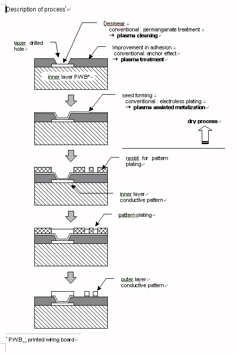
With the development of more powerful mobile phones and other telecommunication equipment, the speed of operating clocks in the semiconductors used in these devices has been continuously increasing, allowing higher integration density of microchips. In order to meet demand from the market, the four companies listed above have been promoting the development of technology allowing higher semiconductor density and higher clock speed in various fields such as materials, equipment and process technologies. As a result, a multi-layer build-up board has been created for high-speed and high-density packages (SUMITOMO's Multi Layer Enhanced by Additive and Plasma Process), under the trade name of Addplap. This product offers higher reliability due to the achievement of excellent high frequencies and higher packaging densities, and industry-first application of dry process to a processing technology, and has the potential to support much higher densities.
The following materials, equipment and process technologies were developed
Materials: Conventional BCB (benzoncylobutene) resins were known to have excellent high frequency properties, but be difficult to machine. Sumitomo Bakelite Co., Ltd. however has now processed these resins using its own advanced technology for organic materials to develop insulating layer materials easily processed using a UV laser micro via technique. These materials have proved superior in terms of high frequencies, achieving specific inductive capacity of 2.7* (as opposed to 4.0 or more for existing materials) and a dielectric loss tangent of 0.0024* (as opposed to 0.0200 or more for existing materials).
*These values represent results achieved, not guaranteed performance
Equipment: Sumitomo Heavy Industries, Ltd., has developed a high-precision UV laser drilling device for micro via processing, as well as plasma treatment and plasma metal deposition systems able to form fine thin-films directly on BCB resins without causing any deterioration in their material properties, based on FPD manufacturing equipment technology.
Processing: Sumitomo Metal Mining Co., Ltd., and Shinko Co., Ltd. have developed a processing solution for a f50 µm-top diameter micro via and a LS=30/30µm line width/space, using their own processing techniques. The two companies will now promote the development of sophisticated technologies for the realization of a f30µm micro via and LS=15/15µm. The new processing technology offers excellent adhesion strength and reliable insulation via greater use of dry process
Shinko Co., Ltd. will establish a mass production system for these products to market them
Shinko specializes in the development, production and marketing of boards for audio-visual, IT and office automation equipment and automobile parts, in its capacity as a general manufacturer of multi-layer printed wiring boards. In order to meet the high performance requirements of rapidly evolving packaging, the company has been developing the ASTOB (Advanced Super Thin Organic Board) and F3s (Fine For Flip-chip Substrate) and producing these products on an increased scale aimed at the CSP and MCM markets
Contact:
Shukichi Takii
General Manager of Research & Development Dept. Director
Shinko Co., Ltd.
Tel / +81-265-79-1811 Fax /+81-265-79-1362
mailto:Shuukichi_Takii@el.smm.co.jp