 |
|
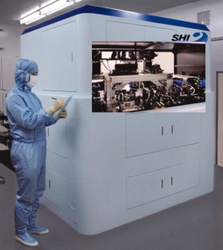
The double-pulse laser annealing system with two solid-state green lasers were developed. Using this system, innovative laser annealing processes for LTPS TFT (Low Temperature Poly-Si Thin Film Transistor) of LCD(Liquid Crystal Display) and for high performance power transistor, IGBT (Insulated Gate Bipolar Transistor) were developed. The double-pulse method is the technique where two lasers are irradiated with the delay time of several hundred nano seconds between them. The system is characterized by the high pulse energy stability of 0.5 % and the precise delay time control with less than 3 % fluctuations to the laser pulse width. They help to effectively control the time evolution of process temperature, which contributes to the improvement of device performances. Applying this technique to the crystallization process of poly-Si films for LTPS TFT, high field effect mobility of 600cm2/Vs comparable to that of single crystal TFT was obtained. And for the backside activation annealing process of IGBT, a deep pn junction of 1.8μm with high activation ratio of more than 80 % were obtained without thermally damaging the circuit elements on the front face.
|
|